Here, we’ll try to test the Nano board and the GOWIN software with a minimal amount of work.
The first step is to plug a USB-C cable into the Nano board.
Under Windows, the board will show up as a COM port and
an LED should repeatedly blink green, blue, red, blank, ... over a period of two seconds.
(The Nano comes configured with a bitstream in flash that blinks the LED.)
Next, download an existing design example from Sipeed’s repository:
git clone https://github.com/sipeed/Tang-Nano-examples.git
(If you don’t want to use git, then you can just download a zip archive.)
Then, go into the Tang-Nano-examples\example_led\led_prj directory and double-click the led_prj.gprj file.
This will load the project into the GOWIN EDA software:
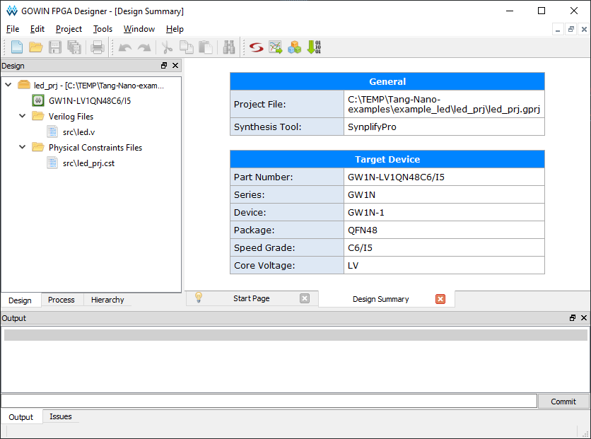
This project is for an RGB LED blinker that is similar to the design that is currently running on the Nano board.
In the Design tab, you can see the led.v Verilog file that describes the behavior of the LED blinker,
and the led_prj.cst constraints file that assigns I/O signals in the Verilog code to specific pins of the FPGA
such as the ones connected to the RGB LED.
Double-clicking either file will show you their contents.
Our first test is to compile this design and load it into the Nano board.
Click on the Process tab and the compilation steps will appear:
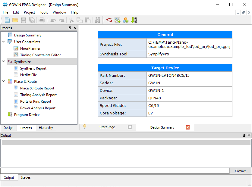
Since the Verilog code and constraints are already there, we’ll mainly be interested in the following steps:
- Synthesis where the Verilog code is translated into logic gates and registers that perform the functions in the code;
- Place & route where the gates and registers are distributed across the logic resources of the FPGA and then wiring is routed to connect their inputs and outputs;
- Program Device where the bits encoding the placed-and-routed circuitry are streamed into the physical FPGA device.
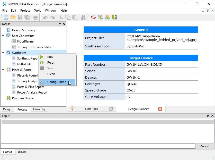
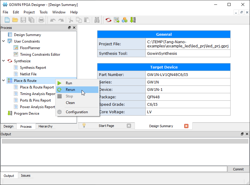
Starting with the synthesis step, first right-click on the Synthesize step and
select Configuration:
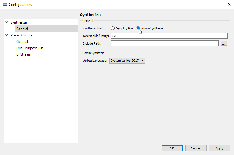
The Gowin EDA software supports two different synthesizers:
Synplify Pro and GOWIN’s in-house synthesizer.
Since we didn’t install the Synplify Pro license when we were setting up the software,
we’re going to use GOWIN’s synthesizer.
In the Configurations dialog window, select GowinSynthesis.
Then click OK and return to the main window.
Now we can generate the FPGA bitstream.
Just right-click on the Place & Route step and select Rerun.
This will initiate the synthesizer and then the place & route steps.
Upon completion, you will see green checkmarks by the synthesis and place & route steps and a bunch of info about the progress of the compilation in the lower pane:
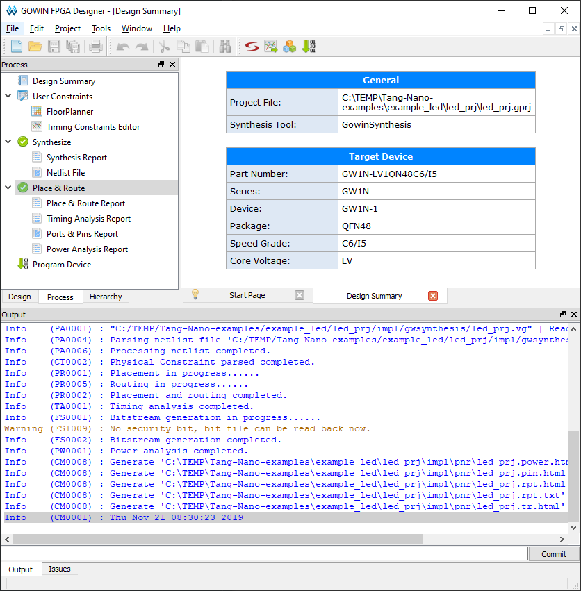
One of the progress items will be Bitstream generation completed.
That means there’s a bitstream available to download into the Nano board’s FPGA.
To do that, double-click the Program Device step and the following dialog will appear:
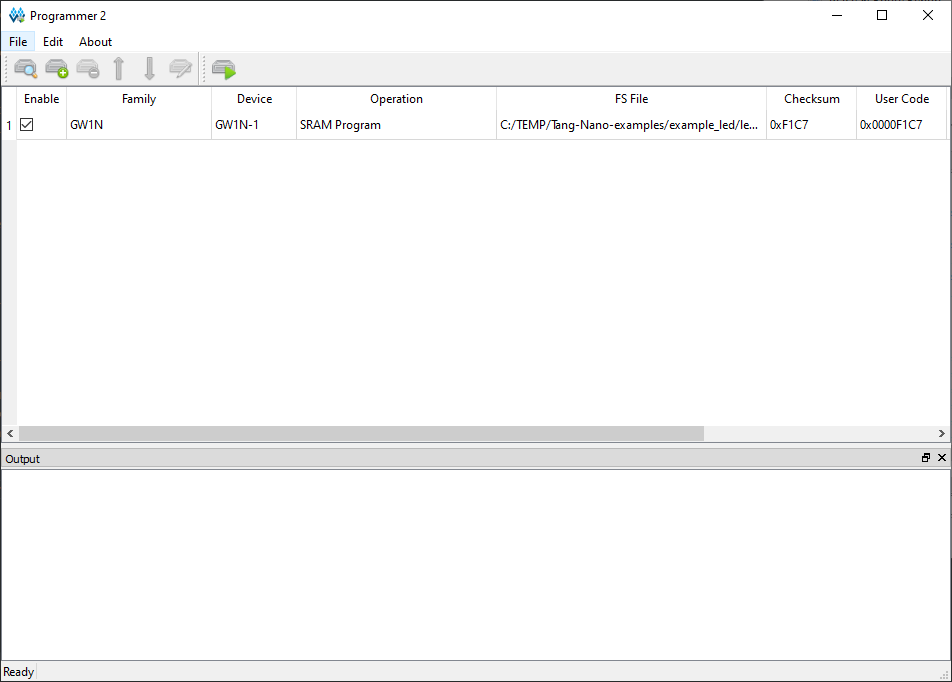
The FPGA can store its bitstream in several ways: in its internal static RAM (volatile),
or it’s internal flash (nonvolatile), or an external flash, or from an external device
via an SPI bus.
We need to tell the device programmer which of those methods to use.
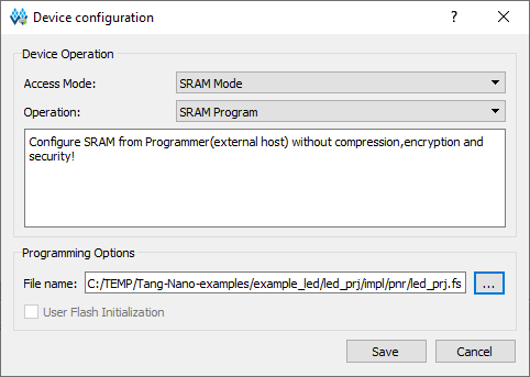
To do that, right-click on the first entry in the list and select Configure Device:
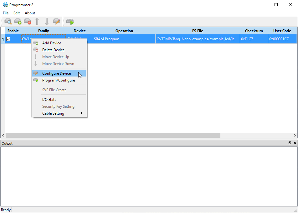
Then in the Device configuration dialog, select SRAM Mode and SRAM Program
so the bitstream will be stored in the FPGA’s internal static RAM.
(SRAM programming is faster than programming the flash and, besides, we don’t want to keep
this design around for very long anyway.)
Then click the Save button.
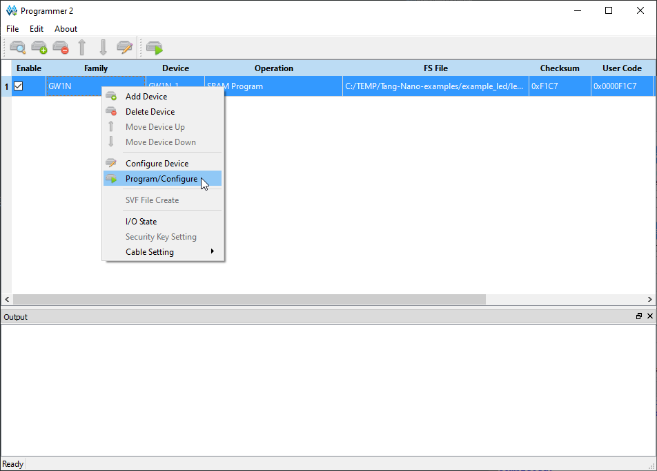
Upon returning to the previous dialog, right-click on the first entry and select Program/Configure.
This initiates the transfer of the bitstream from your PC through the USB cable into the FPGA’s SRAM.
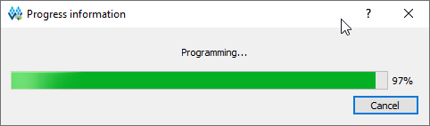
A progress bar will appear to track the transfer, but it won’t be around very long:
After the bitstream is transferred to the FPGA you should see … well, it’s not really any different!
That’s because the design we compiled is not really different from the one that was preloaded into
the Nano’s flash.
That makes it hard to tell if our bitstream works or not.
In order to be sure, we’ll need to change the code so the LED blinks differently.
Close the Programmer dialog window and then go back to the Design tab and
double-click the led.v file to open the Verilog editor:
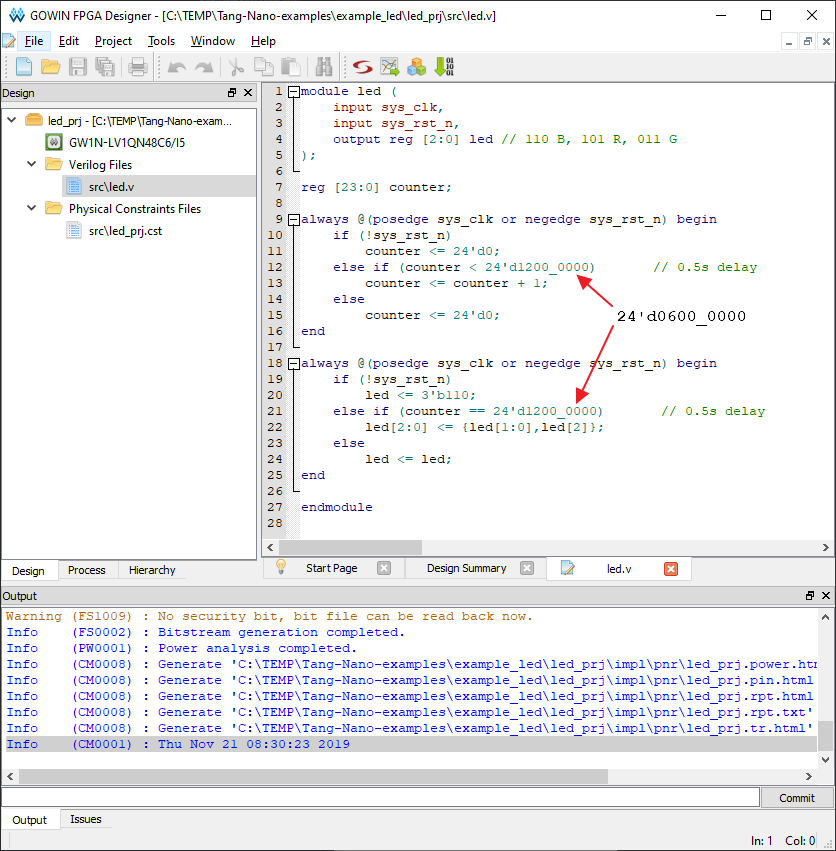
Change the two instances of 24'd1200_000 to 24'd0600_000.
This will halve the duration of each phase of the red, green, blue sequence so it will cycle faster.
Save the updated Verilog file, switch over to the Process tab, and double-click the
Place & Route step to recompile the new code into a bitstream.
Then double-click the Program Device step and reload the FPGA’s SRAM with the new bitstream.
(You won’t need to select the SRAM as the destination for the bitstream: the software will
remember that from last time.)
Upon receiving the new bitstream, the LED on the Nano board should cycle through the colors twice as fast: