Before you can go somewhere new, you gotta know where you are.
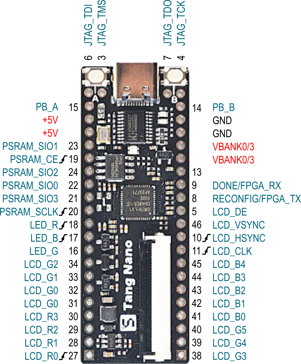
In the previous post, I compiled and downloaded an existing example design to verify that the GOWIN EDA software was working. But to create new designs of your own, you’ll need to know what the pins of the FPGA are connected to on the Nano board. (For example, what FPGA pins are connected to the two pushbuttons?) That information is contained in the Nano board schematic, but getting it in a useful form requires you to trace the wiring from the FPGA pins to other parts on the board. Even with a small schematic, that’s more painful than it should be.
To make it a bit easier, I created a spreadsheet that lists where the FPGA pins are connected. It also includes a board image showing where the FPGA pins exit the board through the 0.1”-spaced prototyping headers.