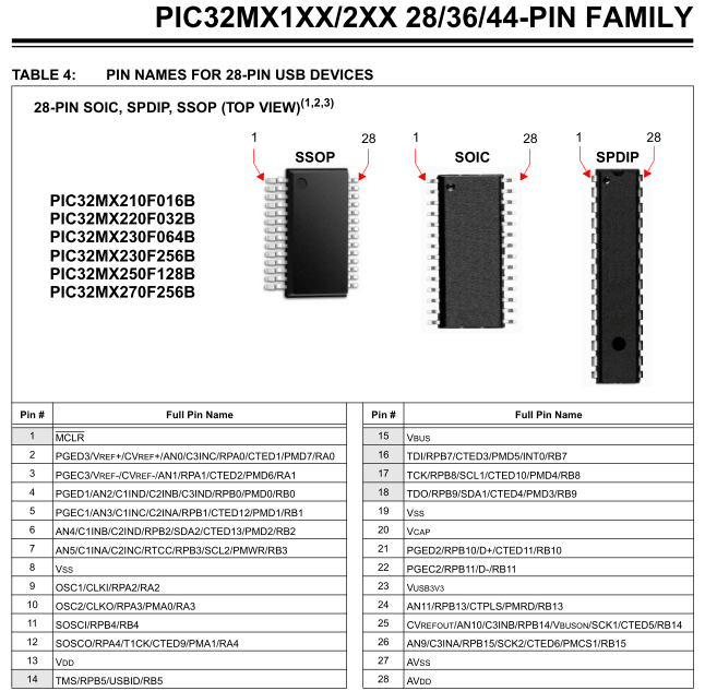
In my previous post, I showed how to use SKiDL to describe the circuit for a simple USB-to-JTAG interface circuit. That circuit used a PIC32MX microcontroller in a 28-pin SSOP package:

and the corresponding SKiDL code was:
pic32 = Part(pic32_lib, 'pic32MX2\*0F\*\*\*B-SSOP28-SOIC28-SPDIP28',
             footprint='Housings_SSOP:SSOP-28_5.3x10.2mm_Pitch0.65mm')
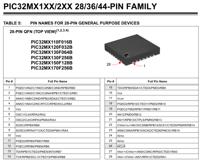
I wanted to try using the same processor, but housed in a smaller QFN package:

To do that, I changed the SKiDL code to reference a different part and footprint like this:
pic32 = Part(pic32_lib, 'pic32MX2\*0F\*\*\*B-QFN28',
             footprint='Housings_DFN_QFN:QFN-28-1EP_6x6mm_Pitch0.65mm')
That's it! No other changes were needed because I wrote my SKiDL code to use
pin names instead of pin numbers.
For example, I connected the 12 MHz crystal to the microcontroller OSC1 and OSC2
pins like this:
pic32['OSC1, OSC2'] += xtal[3, 1]
This works for either version of the microcontroller because they both have
pins named OSC1 and OSC2.
But, if I had made the crystal connections for the microcontroller in the 28-pin SSOP
using pin numbers:
pic32[9,10] += xtal[3, 1] # OSC1==9, OSC2==10 for 28-pin SSOP version.
then I would have had to change the code when I switched to the QFN packaged version of the microcontroller:
pic32[6,7] += xtal[3, 1] # OSC1==6, OSC2=7 for 28-pin QFN version.
Multiply this by the number of pins a device has (which can be over a thousand for modern-day parts like FPGAs), and you can see how using pin names reduces the effort and likelihood of errors when making a design change.
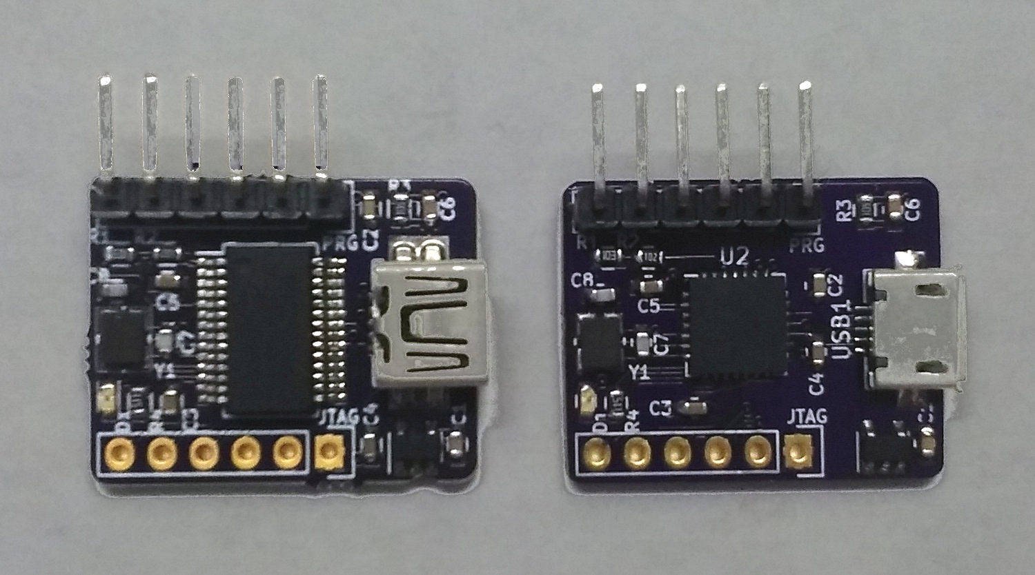
For the new board, I also changed from using a mini USB connector:
usb_conn = Part(xess_lib, 'USBB', footprint='XESS:UX60SC-MB-5ST')
to a micro connector:
usb_conn = Part(xess_lib, 'USB-MicroB', footprint='XESS:USB-microB-1')
Once again, using pin names meant I didn't have to touch the rest of the code:
usb_conn['D\+, D-, VCC, GND, NC'] += pic32['D\+, D-'], vusb, gnd, NC
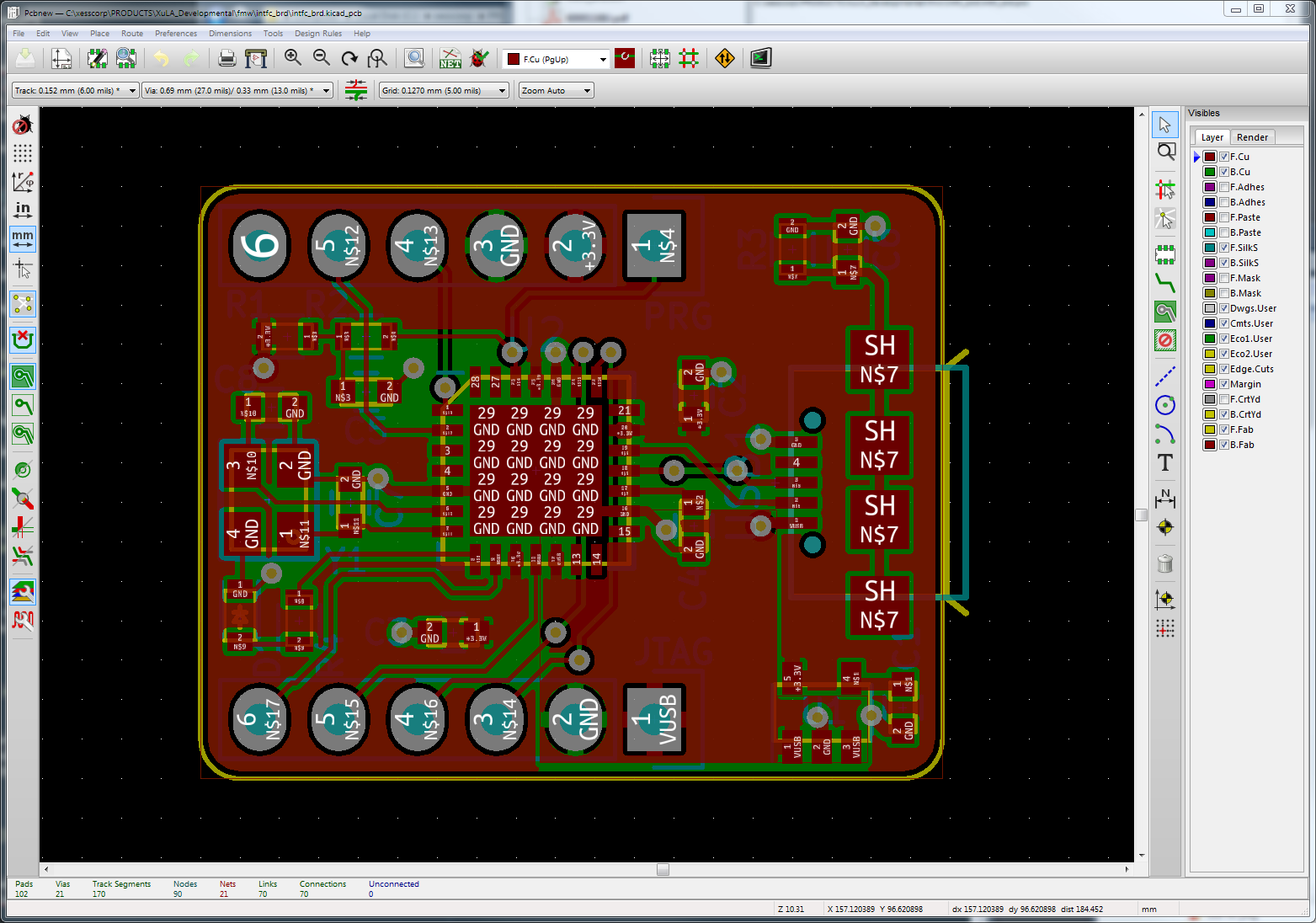
After the changes to the SKiDL script were done, I just ran it and imported the
netlist into KiCad's PCBNEW layout program.
At that point, it didn't matter whether I used pin names or numbers: I still had
to re-route the wire traces on the PCB because the physical location
of the pins had changed. There's no getting around that.

Here's a side-by-side of the previous and new USB-to-JTAG boards:

